Chapter 04 · Watch, then practise
Microprocessor System
Watch the related lecture, then read the question and answer below.
21 questions · 6 playlist videos. Matches are based on video titles; broader background matches are labeled.
Watch the full playlist ↓Chapter playlist
Microprocessor System
Address Decoding
AAkrit Subedi · 15:43
Related address-decoding lecture from the supplied chapter playlist; this is a topic match, not a verified solution to this exact question.
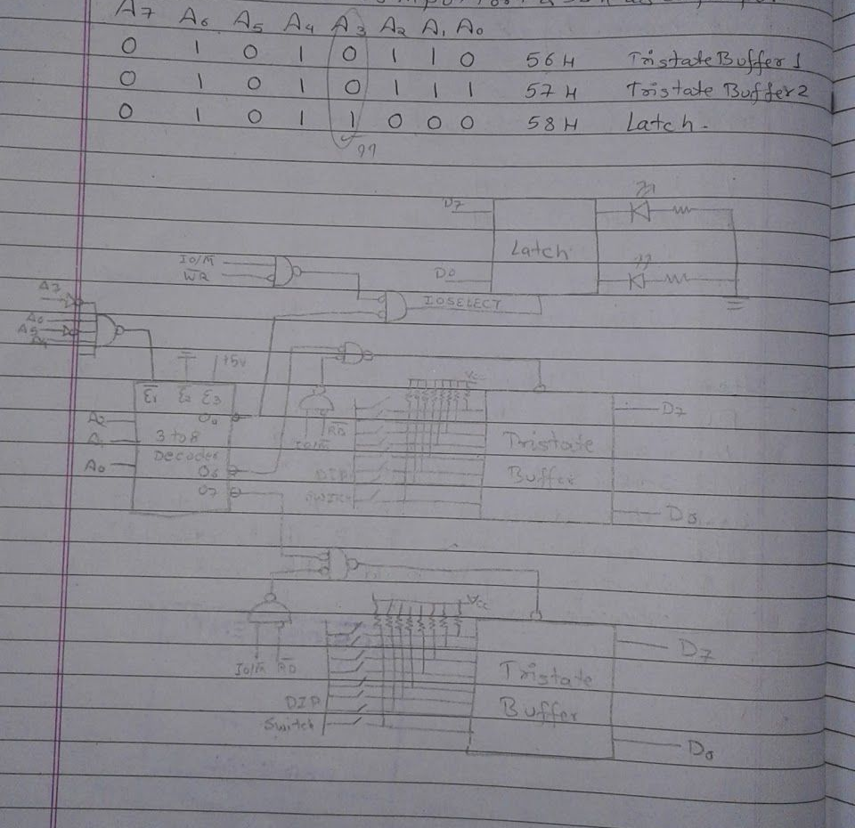
1. Input ports 56H and 57H; output port 58H
Design an interfacing circuit with 8085 to make 56H & 57H as input Port & 58H as output port.
Answer
Address Decoding
AAkrit Subedi · 15:43
Related address-decoding lecture from the supplied chapter playlist; this is a topic match, not a verified solution to this exact question.
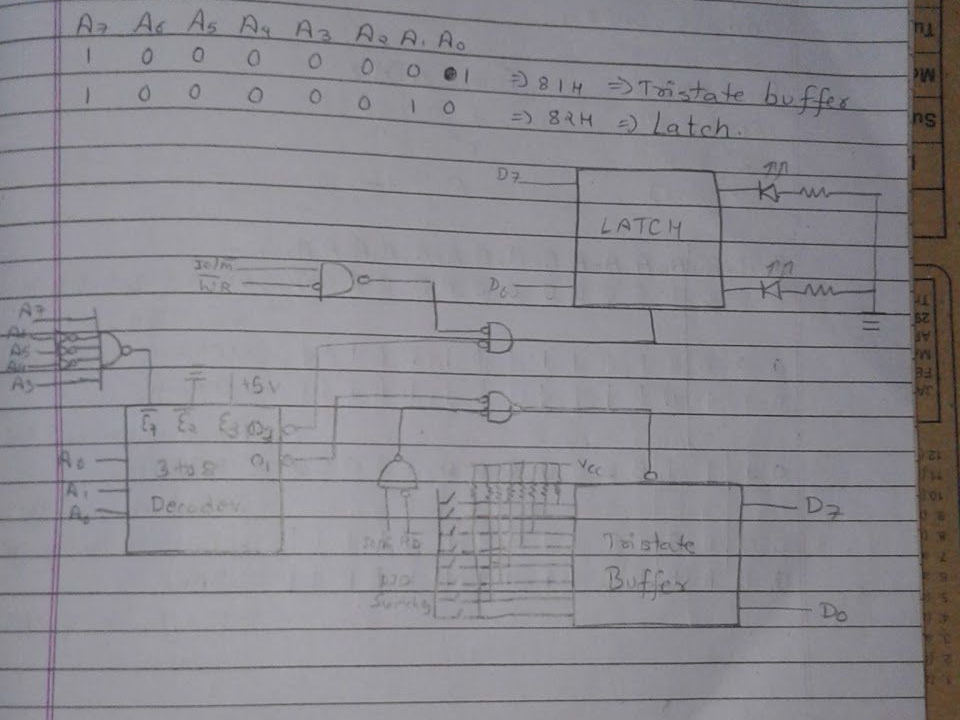
2. Input and output ports at 81H and 82H
Design the address decoding interface of an input port & output port for 8085 at 81H & 82H address.
Answer
Address Decoding
AAkrit Subedi · 15:43
Related address-decoding lecture from the supplied chapter playlist; this is a topic match, not a verified solution to this exact question.
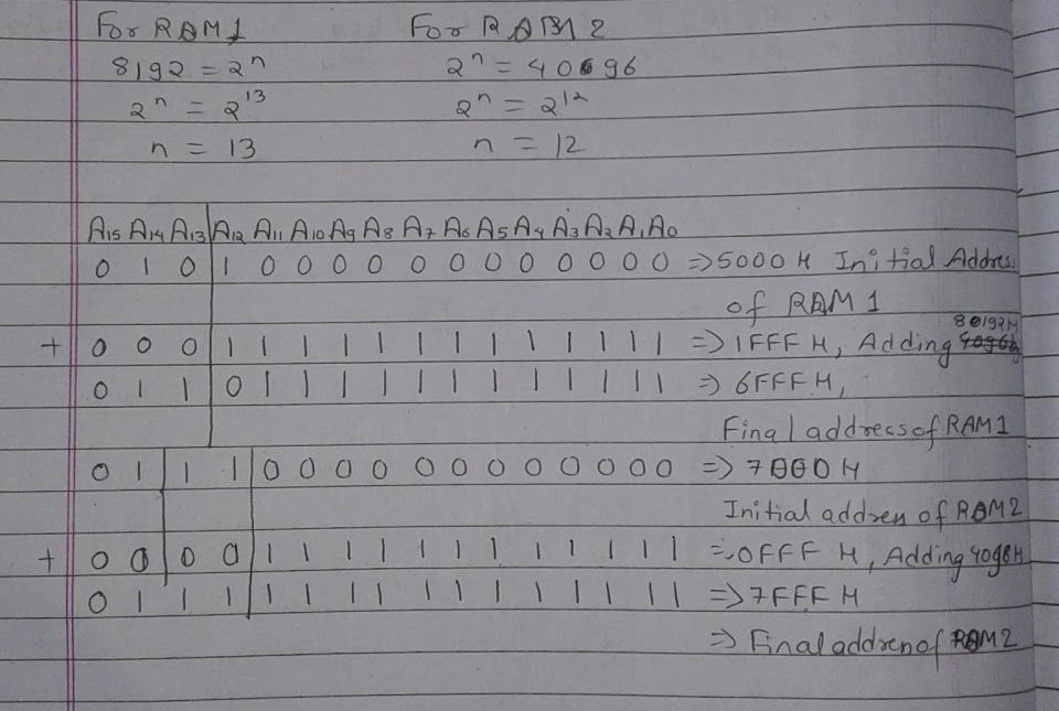
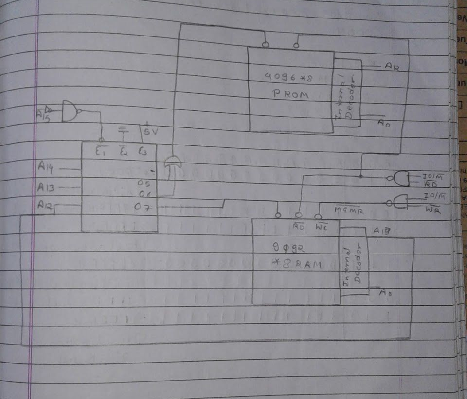
3. 8192 × 8 RAM and 4096 × 8 PROM
Present an address decoding circuit to handle one 8192*8 RAM chip & one 4096*8 PROM chip with 8085 starting consecutively at address 5000H.
Answer
Address Decoding
AAkrit Subedi · 15:43
Related address-decoding lecture from the supplied chapter playlist; this is a topic match, not a verified solution to this exact question.
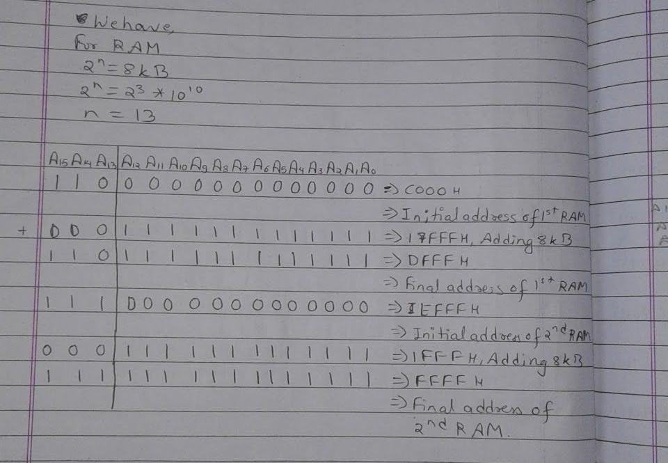
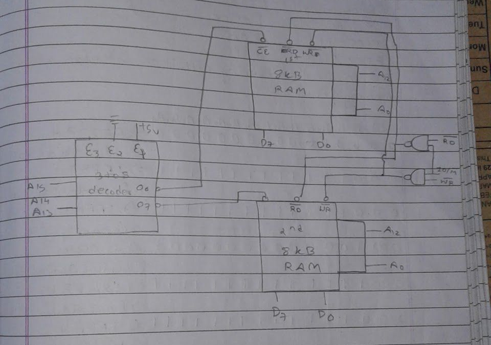
4. Two 8kB RAM memory blocks
Draw the address decoding circuit to interface two RAM memory block each of 8kB at address C000H.
Answer
Address Decoding
AAkrit Subedi · 15:43
Related address-decoding lecture from the supplied chapter playlist; this is a topic match, not a verified solution to this exact question.
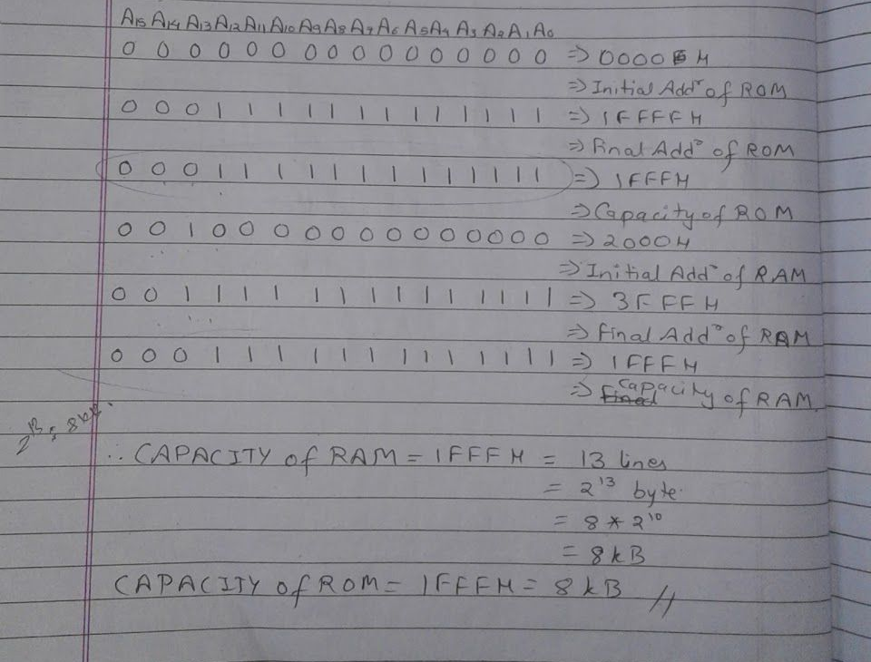
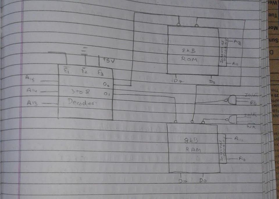
5. Memory capacity and interfacing
Determine the capacity of devices in the following memory range.
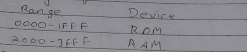
Design an interfacing circuit to interface above memory device.
Answer
Address Decoding
AAkrit Subedi · 15:43
Related address-decoding lecture from the supplied chapter playlist; this is a topic match, not a verified solution to this exact question.
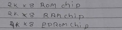
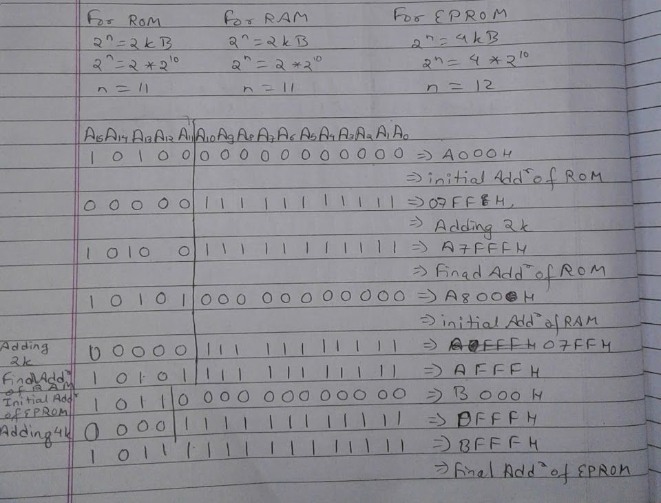
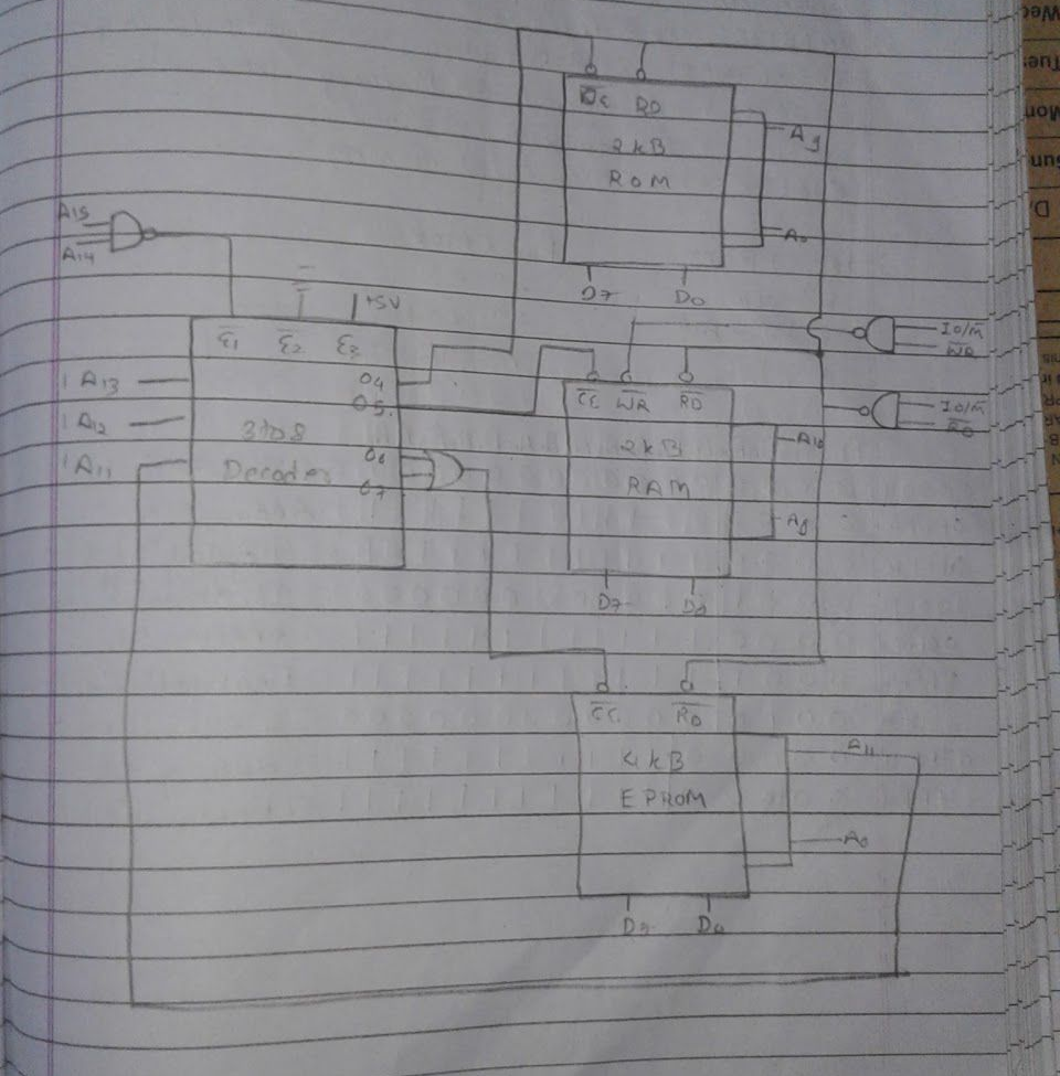
6. Memory units with a 74LS138 decoder
With neat diagram explain the interfacing circuit using a 3:8 decoder (74LS138) needed to connect the following memory units to 8085 microprocessor consecutively starting from memory location A000H
Answer
Address Decoding
AAkrit Subedi · 15:43
Related address-decoding lecture from the supplied chapter playlist; this is a topic match, not a verified solution to this exact question.
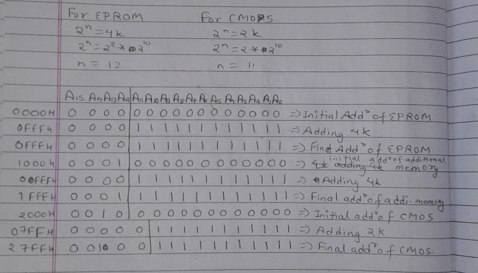
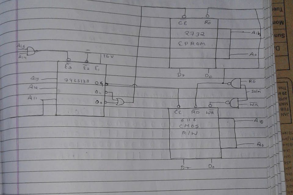
7. 2732 EPROM and 6116 CMOS memory
Design an interfacing circuit for following problem
i) 74LS138: 3 to 8 decoder
ii) 2732(4k*8): EPROM address range should begin at 0000H & additional 4k Memory space should be available for future explanation.
iii) 6116(2k*8): CMOS R/W memory.
Answer
Address Decoding
AAkrit Subedi · 15:43
Related address-decoding lecture from the supplied chapter playlist; this is a topic match, not a verified solution to this exact question.
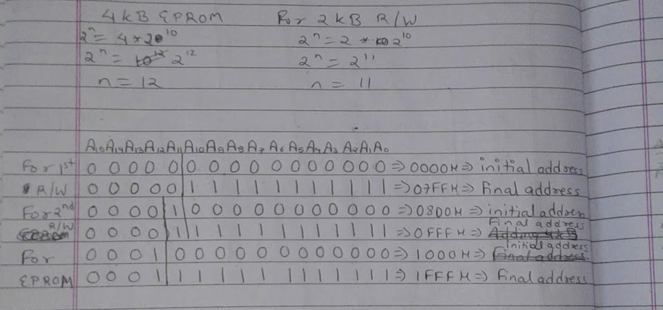
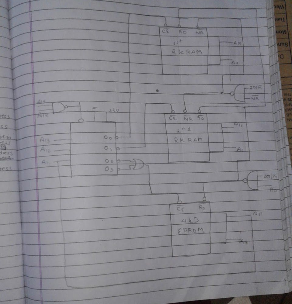
8. One 4kB EPROM and two 2kB R/W memories
Design an interfacing circuit to interface one 4kB EPROM & two 2kB R/W memory.
Answer
No dedicated 8255 PPI or parallel-interfacing lecture is listed in the supplied chapter playlist.
9. Parallel data transfer and 8255 PPI
What are the different ways in which parallel data are transfered? With help of block diagram of 8255 PPI, explain its uses in parallel interfacing.
Answer
The different ways in which parallel data are transferred are:-
i) Simple input & output
In this form of data transfer, no coordinating signals are used to output the data. Microprocessor simply put the data bus & the device address on address bus.
ii) Simple strobe input/output.
In simple strobe input/output, an external device asserts its STB signal low when valid data is present.
iii) Single handshake I/o
In simple strobe I/o, the sending device doesnot know when it is safe to send next data byte. This defficiency is removed in single handshaking I/o by using ACK signal to determine whether the receiving device is ready to accept the data or not.
Double handshaking I/o
In a situation where highly coordinated transfer of data is required, double handshake I/o is used.
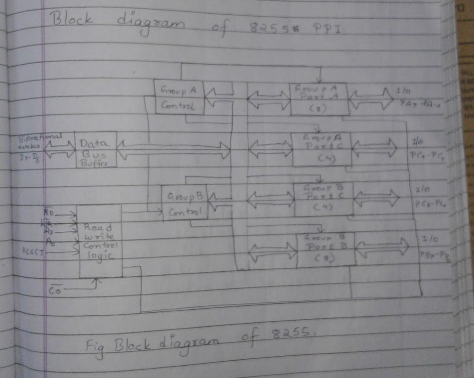
There are eight data lines buses where 8 bytes of data can be handled simultaneously by this bus and on each port and on the links to the device. So 8255 PPI make use of parallel interface.
No dedicated 8255 control-word lecture is listed in the supplied chapter playlist.
10. 8255 control words in I/O and BSR modes
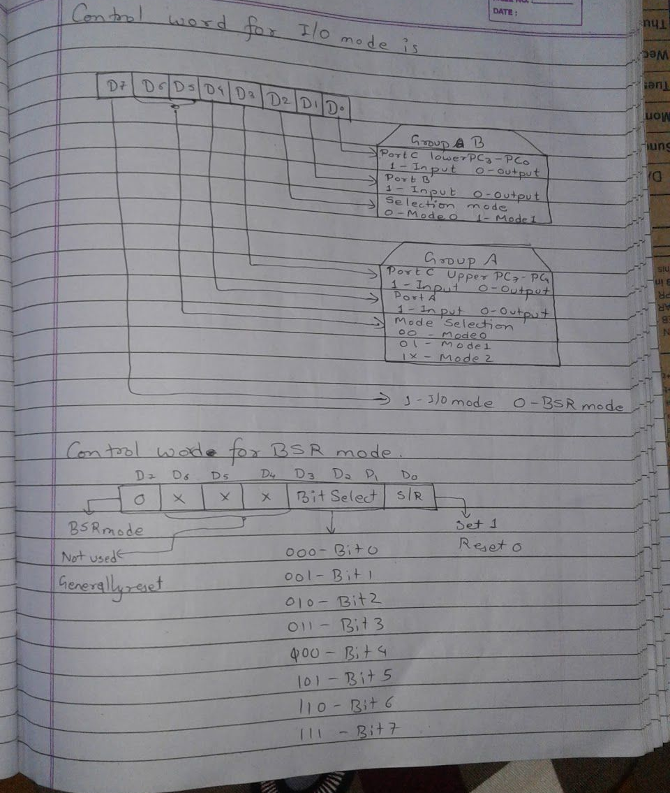
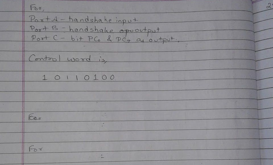
How Control words are defined for 8255 in both I/o and BSR mode. Write Control word for:-
a) Initialize an 8255 as: Port A - Handshake input, Port B - handshake output, Port C - bits PC6 and PC7 as outputs.
b) To set and reset bit PC3 and PC5 used for initializing Port A and Port B interrupt request respectively.
Answer
No dedicated serial communication or RS-232C lecture is listed in the supplied chapter playlist.
11. Synchronous, asynchronous and RS-232C communication
What is Synchronous & Asynchronous Communication. Describe RS-232C standard & its handshaking signals for serial communication.
Answer
Synchronous Communication
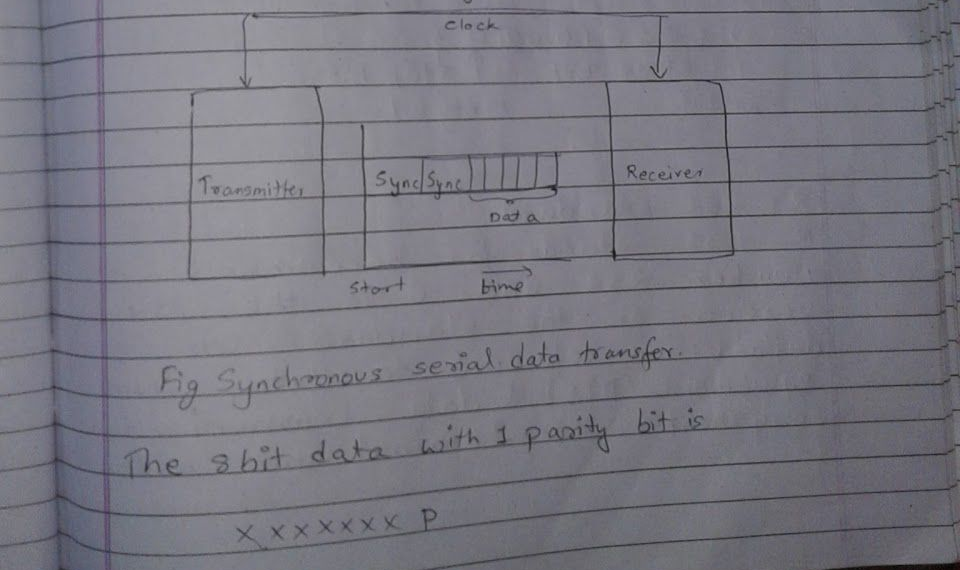
In synchronous communication, one or more additional data signals are transmitted along with data bits. This signal indicates when the next bit is valid on the data lines. These signals are formed either by a clock signal or by handshake signal of request or acknowledge.
Asynchronous Communication.
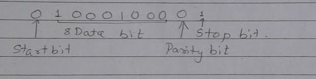
Here both the transmitter and the receiver must be operated at the same clock frequency. The transmitter sends the formatted data unit when it is ready for the transmission. This data unit call a serial data unit (SDU), which serves as a synchronizing agent between the receiver & transmitter. An SDU consists of one start bit, Data bit, parity bit & finally a stop bit: as.
RS 232 standard
RS 232 stands for Recommend standard number 232 and C is the latest version of the standard. It is defined in reference to data terminal equipment (DTE) & data communication equipment (DCE) - Terminal and modem.
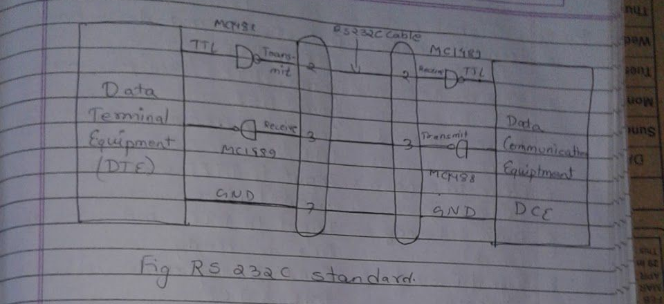
The rate of data transmission in RS232C is restricted to a maximum of 20kBaut and a distance of 50 feet.
The signal levels of RS232C are not compatible with that of the DTE and DCE, which are TTL signals. Hence TTL to RS232C and RS232C to TTL conversion are required for establishing link between DTE and DCE.
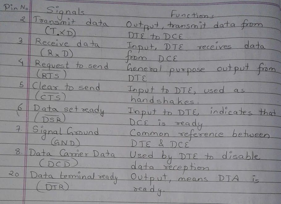
Among 25 pins of RS232C, Some of them can be listed below with their functions:
Address Decoding
AAkrit Subedi · 15:43
Related address-decoding lecture from the supplied chapter playlist; this is a topic match, not a verified solution to this exact question.
12. Address decoding and mapped I/O
What do you mean by address decoding? What is memory I/o and IO mapped I/o? Why the number of out ports in the peripheral-mapped I/o is restricted to 256 ports?
Answer
Address decoding
A microcomputer has a microprocessor memory and i/o devices attached. A processor communicates with all parts interconnected in the system through common address & data bus. Hence, only one device can transmit data through the bus at a time & others can only receive data. If more than one device attempt to send data through the bus at the same time, the proper communication among the devices does not become possible because the data sent by them gets garbled.
To avoid this situation, ensuring that the proper device gets address at proper time, the technique address decoding is used.
Memory mapped I/o
In memory mapped I/o method of Address decoding, the I/o devices are addressed with 16-bit address. It means that in this mode, the chip select signal for the devices are derived from using all the 16 address lines from the processor.
I/o memory mapped I/o
In I/o mapped I/o, the I/o devices are addressed with 8 bit address. It means that chip selects signal for the devices are derived by using the 8 address lines (A8-A15) are unused & considered donot care condition.
Address Decoding
AAkrit Subedi · 15:43
Related address-decoding lecture. The supplied playlist does not include a dedicated single/double-handshaking lecture.
13. Handshaking and two 8k × 8 ROM chips
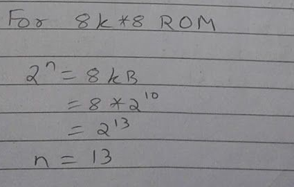
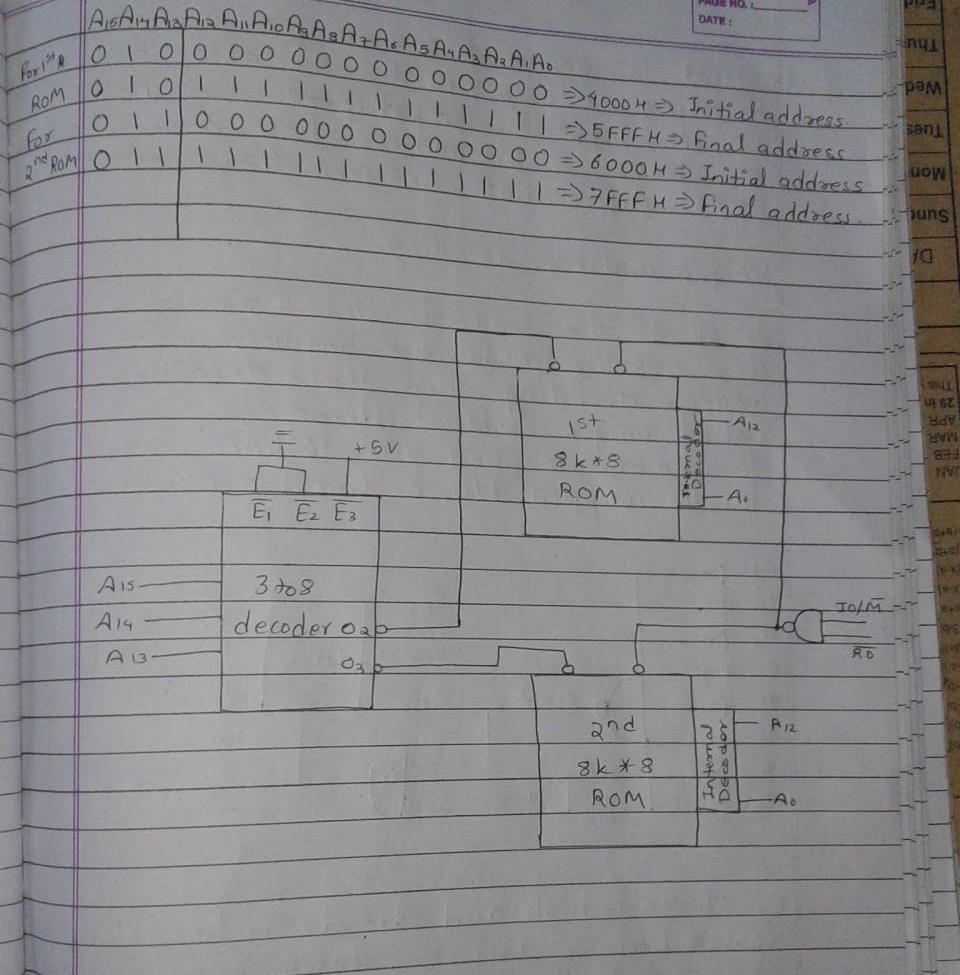
Explain single handshaking and double handshaking technique used in parallel interfacing with a microprocessor? Design an address decoding circuit to interface two 8k*8 ROM chips at addressing starting at 4000H.
Answer
Single handshake I/o.
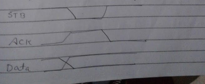
The pheripheral outputs some parallel data and sends STB signal to the microprocessor. The STB signal is the signal from the pheripheral to the microprocessor to indicate that the peripheral is ready to transmit the valid data to the microprocessor. The microprocessor detects the STB signal on a polled or interrupts basis and reads in the byte of data. The microprocessor then sends an ACK signal to the peripheral to indicate that the peripheral can send the next byte of data. From this viewpoint of microprocessor, this operation is referred to as single handshake.
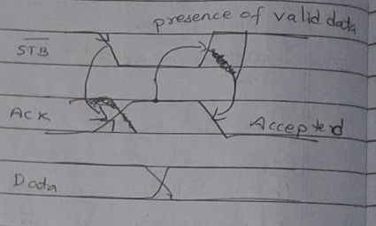
Double handshaking I/o
Here sequence of operation are:-
Sending device STB signal low to ask if the receiving device is ready to receive the data or not.
Receiving device asserts its ACK signal high to indicate its readiness to receive data.
Sending device then puts the data & raise its STB signal high to represent the presence of valid data.
The receiving device reads the data and loads the ACK signal to indicate the succesful reception of data.
Address Decoding
AAkrit Subedi · 15:43
Related address-decoding lecture from the supplied chapter playlist; this is a topic match, not a verified solution to this exact question.
14. Unique and non-unique address decoding
What is unique & non-unique address decoding: explain with suitable example. If an input & output port can have the same 8 bit address how does the 8085 differentiate between the ports?
Answer
Non unique address decoding
If all of the address lines are available on the mapped mode are not used for address decoding then that decoding is called non-unique address decoding.
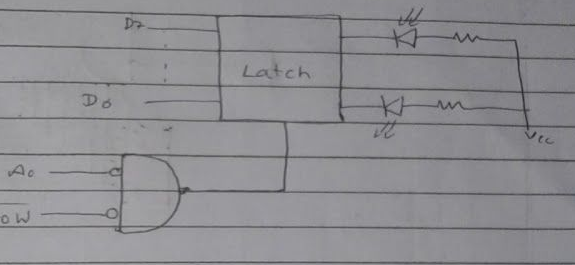
eg. If A0 is low and IOW is low, then latch gets enable. Here A1-A7 is neglected that is any even address will enabled the latch.

Unique address decoding
If all of the address lines available on the mapping mode are the used for address decoding then that decoding is called unique address decoding.
In memory mapped I/o, 16 lines are used & in IO mapped I/o, 8 lines are used.
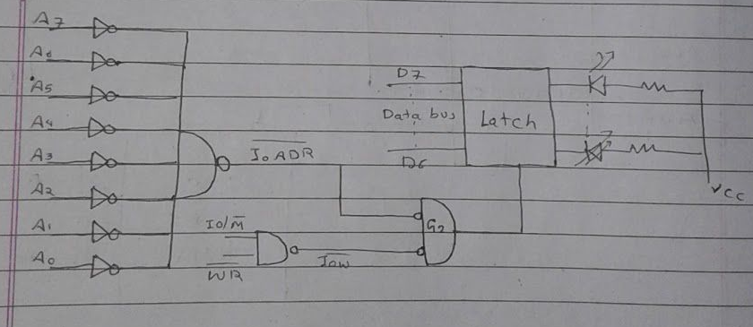
Eg if A0 is high and A1-A7 is low and if IOW becomes low, the latch gets enabled. The data to the LED can be transfered in only one case. Hence device have unique address of 01H.
Introduction to timing diagram
AAkrit Subedi · 6:05
Choose a video · 3 lectures
Related timing-diagram lectures from the supplied playlist. The titles do not identify a worked solution for this exact instruction.
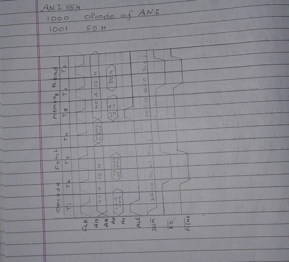
15. Machine cycle, Tstates and ANI 55H timing
What do you mean by Machine cycle & Tcycle Tstates? Draw a time bus timing diagram for a instruction ANI 55H of 8085 microprocessor. Calculate the time required to execute such instruction, if microprocessor is operating at 2MHz clock frequency.
Answer
Machine cycle.
The machine cycle can be do is the total operation of microprocessor which is cat classified as four groups
- OpCode Fetch
- Memory Read and Write
- I/o Read and Write
- Request Acknowlege
Tstates.
Introduction to timing diagram
AAkrit Subedi · 6:05
Choose a video · 3 lectures
Related timing-diagram lectures from the supplied playlist. The titles do not identify a worked solution for this exact instruction.
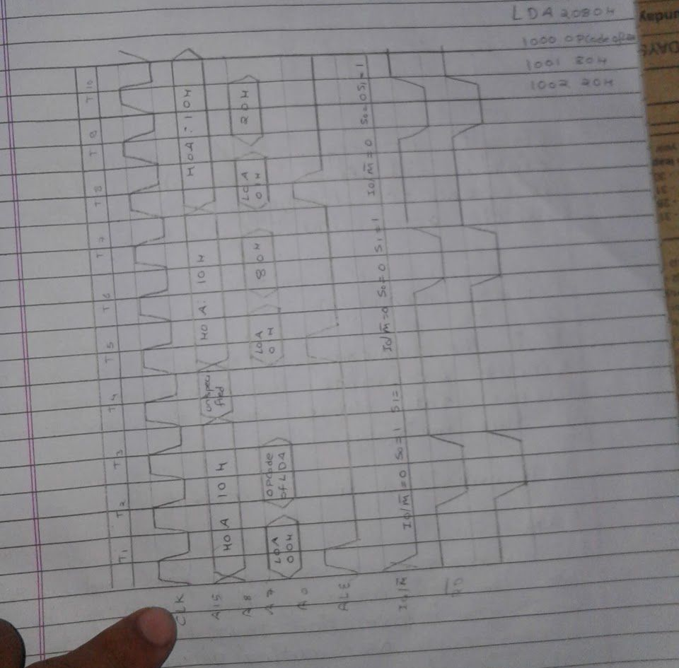
16. LDA 2080 timing diagram
Draw the timing diagram of LDA 2080.
Answer
No dedicated memory hierarchy or access/cycle-time lecture is listed in the supplied chapter playlist.
17. Primary and secondary memory
Classify primary & secondary memory and explain in brief. Discuss about the importance of memory hierarchy. Also explain access time & cycle time.
Answer
Primary memory.
It is the memory used by microprocessor to execute programs. The microprocessor can access only those items that are stored in this memory.
It is classified as: RAM & ROM
RAM
Microprocessor can read from and write into the this memory. This memory is used for information that are likely to be altered such as writing program or receiving data.
ROM
ROM contains permanent pattern of data that cannot be changed.
Secondary memory.
The device that provides backup storage are called secondary memory. It includes serial access type such as magnetic disk tapes and random access type such as magnetic disks. It is non volatile memory.
The importance of memory hierchy are:-
- Memory Hierchy is to obtain the highest possible access speed while minimizing the total cost of the memory system.
- If memory has larger capacity, more applications will get space to run smoothly.

8085 PIN DIAGRAM & DESCRIPTION
COMAT WORLD · 25:01
Topic match: this playlist lecture covers the 8085 pin diagram and description.
18. Logic pin out of the 8085
Draw the logic pin out of 8085 microprocessor.
Answer
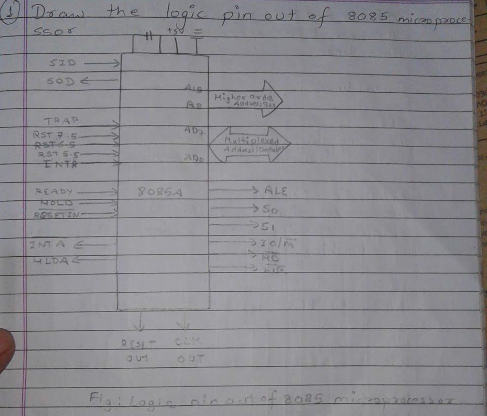
Address pin (A15-A8)
These are used for 8 line pins which exclusively form higher order Addresses (HOA).
Address and Data pins (AD0 - AD7)
These are lower order address pins shared by 8 bit data lines.
Control lines.
ALE
The rising edge of thise Address latch Enable is used to indicate the beginning of instruction.

R̅D̅
This is the READ control tristate output.
WR
This is WRITE control tristate output.
READY
READY pin is used by slower external device for obtaining extra time to communicate with 8085
HOLD
HOLD input signal goes high when the external device want to take control of system bus.
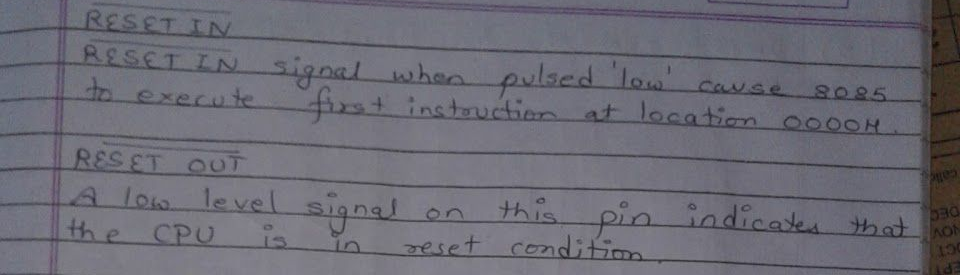
HLDA
The CPU places a logic high on this hold acknowledge output pin to acknowledge that it has received 'HOLD' request & it will release the control of the bus in the next period.
INTA
It is interrupt acknowledge pin.
Interrupt signal
These are TRAP INTR, RST 7.5, RST 6.5, RST 5.5 and INTR in the priority order 0 to 1 to 5.
SID
The serial input data line for serial input/out transfer
SOD
The serial output data lines for serial input/output transfer.
Introduction to timing diagram
AAkrit Subedi · 6:05
Choose a video · 3 lectures
Related timing-diagram lectures from the supplied playlist. The titles do not identify a worked solution for this exact instruction.
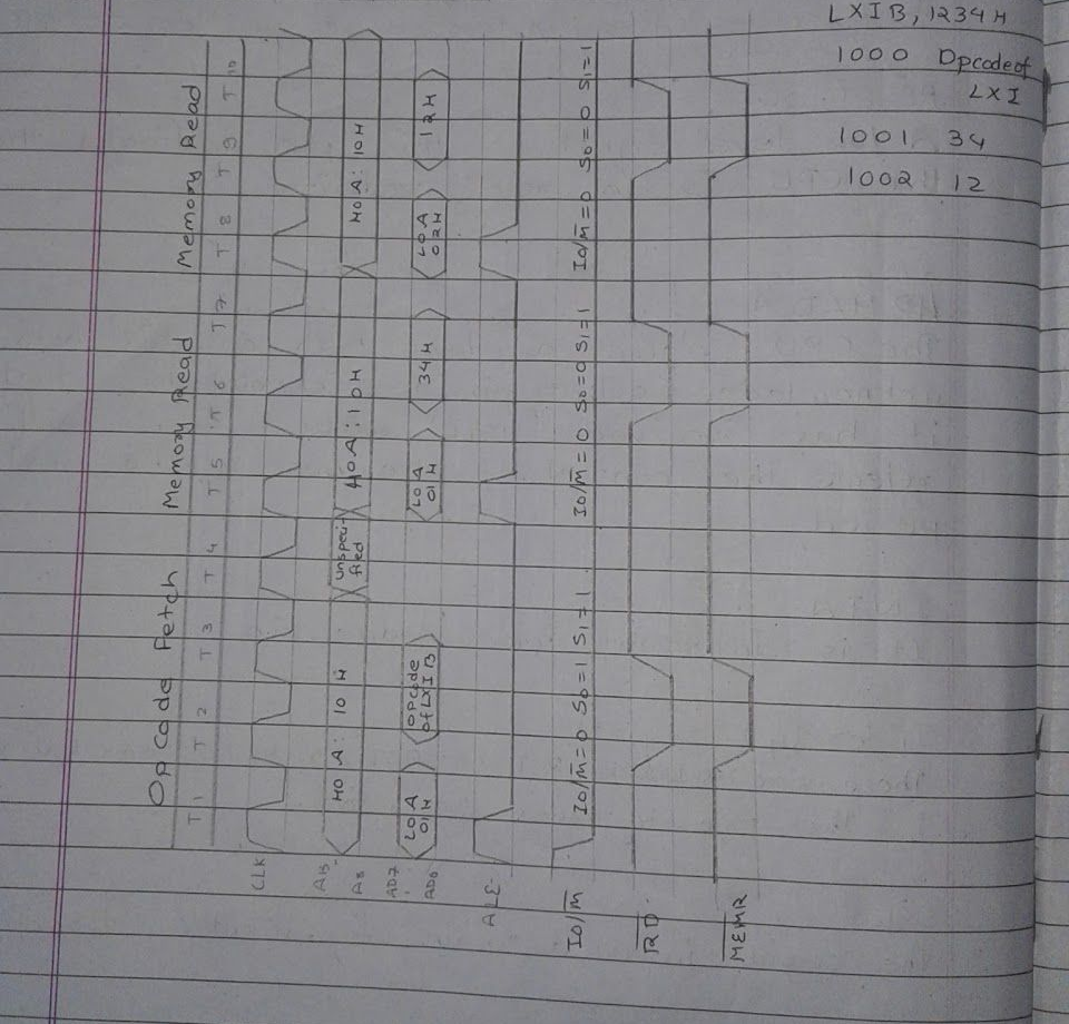
19. LXI B, 1234H bus timing diagram
Draw & explain the bus timing diagram
(i) LXI B, 1234H.
Answer
Introduction to timing diagram
AAkrit Subedi · 6:05
Choose a video · 3 lectures
Related timing-diagram lectures from the supplied playlist. The titles do not identify a worked solution for this exact instruction.
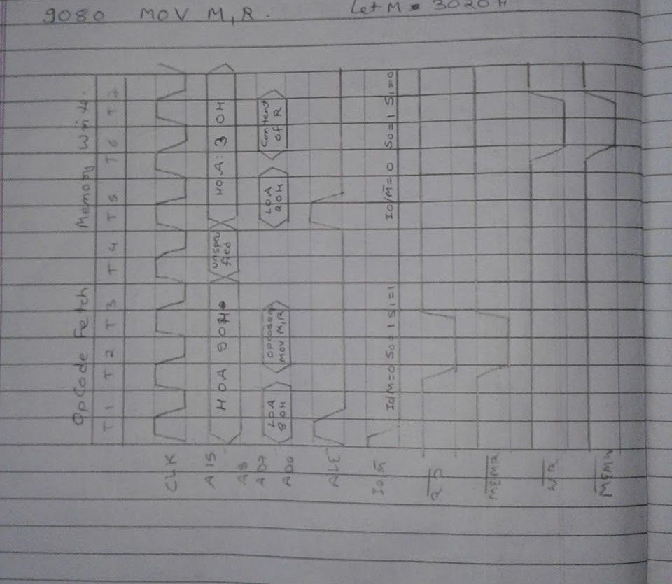
20. MOV M, R timing example
For MOV M, R
Let M = 3020H
Answer
Introduction to timing diagram
AAkrit Subedi · 6:05
Choose a video · 3 lectures
Related timing-diagram lectures from the supplied playlist. The titles do not identify a worked solution for this exact instruction.
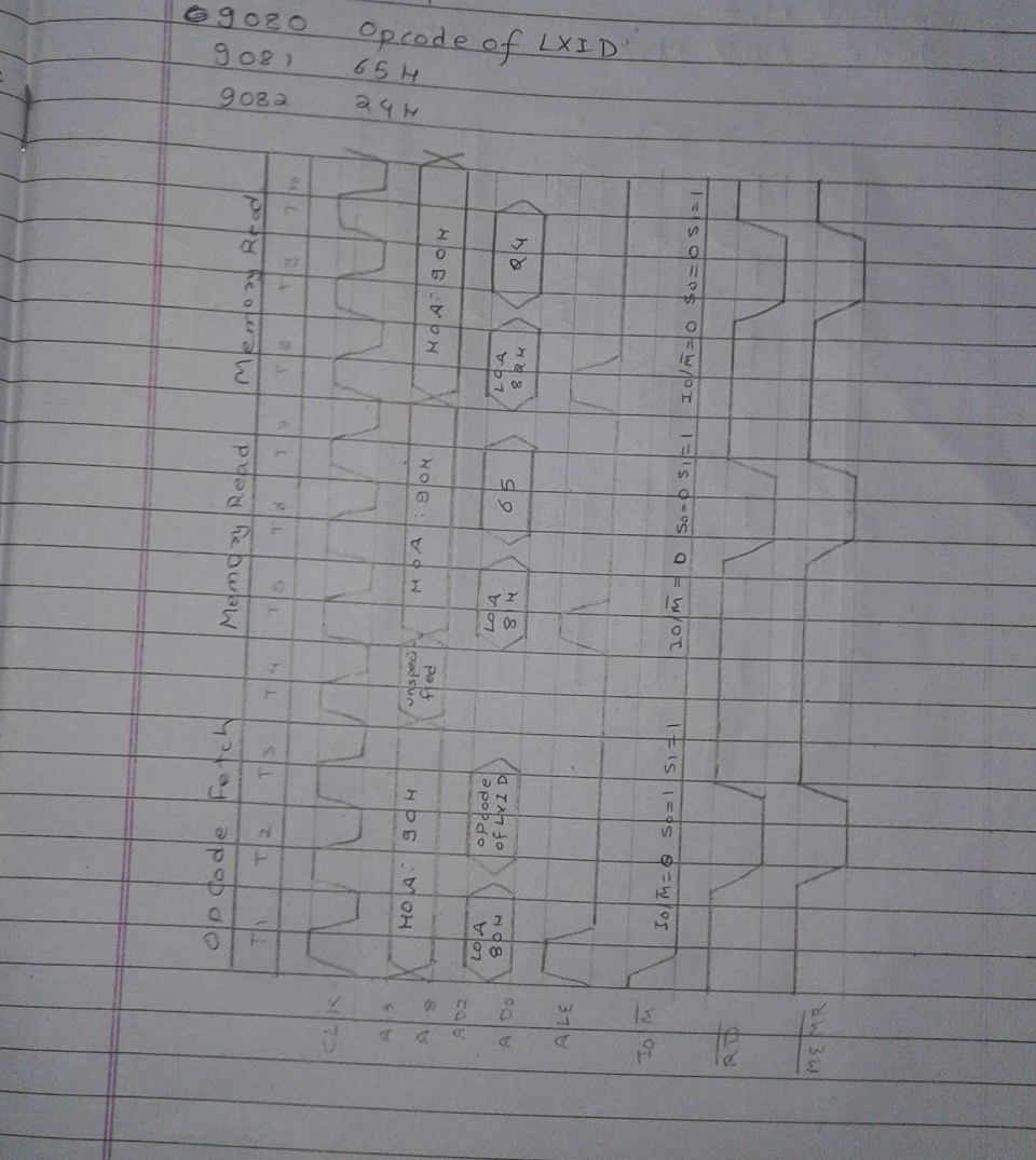
21. LXI D, 2465H timing example
LXI D, 2465H
Answer
More videos from this chapter’s playlist
These playlist videos do not have a direct match among the questions above.
STA 8050H
AAkrit Subedi · 8:12